Journal Papers
[Category: Deep-UV Photonics]
·
Get
the preprints
of papers posted on the arXivs.
·
We
have published in IEEE journals, IEDM/DRC, APL, Science, Nature journals,
Physical Review journals, JAP, Nano Letters, etc.
·
The
complete list of papers below is sorted into categories here:
Highlights of our contributions
to the area of Deep-UV Photonics
7) 2016: Demonstration of sub
230 nm emission from GaN quantized heterostructures for deep-UV LEDs by MBE.
6) 2014: First demonstration of a
tunnel-injection deep-UV quantum-dot LED with polarization-induced
p-type doping.
5) 2013: First demonstration of a tunnel-injection
deep-UV quantum-dot LED.
4) 2011: First demonstration of a N-polar
quantum-well LED with polarization-induced p-type hole injector.
3) 2010: First demonstration of polarization-induced
p-type doping in wide-bandgap semiconductors.
2) 2009: Uncovered the physics of polarization-induced
Zener tunnel junctions in wide-bandgap heterostructures.
1) 2002: First demonstration of polarization-induced
n-type doping in wide-bandgap semiconductors.
2016
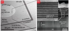
188) Deep-UV Emission from Ultra-Thin
GaN/AlN Heterostructures
(D. Bayerl et al.,
Appl. Phys. Lett., accepted, to appear 2016)
(S. M. Islam et al.,
Jap. J. Appl. Phys., 55, 05FF06 2016)
2015
170) Localized
surface phonon polariton resonances in polar gallium nitride
(K. Feng et al.,
Applied Physics Letters, 107, 081108 2015)
(M. Qi et al.,
Appl. Phys. Lett., 106, 041906 2015)
2014
(J. Verma et al.,
Appl. Phys. Lett., 104, 021105 2014)
2013
114) Tunnel-injection
GaN quantum-dot ultraviolet light-emitting diodes
(J. Verma et al.,
Appl. Phys. Lett., 101, 032109 2013)
2012
87) Charge
transport in non-polar and semi-polar III-V nitride heterostructures
(A. Konar, A. Verma, T. Fang, P.
Zhao, R. Jana, and D. Jena,
Semicond. Sci. Technol., 27, 024018, 2012)
2011
81) N-Polar
III-nitride quantum well light emitting diodes with polarization-induced doping
(J. Verma, J. Simon, V. Protasenko,
T. Kosel, H. Xing, and D. Jena,
Appl. Phys. Lett., 99, 171104, 2011)
74) Stark-Effect
Scattering in Rough Quantum Wells
(R. Jana, and D. Jena
Appl. Phys. Lett., 99, 012104 2011)
68) Polarization
Engineering in Group-III Nitride Heterostructures: New Opportunities for Device
Design
(D. Jena, J. Simon, K. Wang, Y. Cao, K. Goodman, J. Verma, S.
Ganguly, G. Li, K. Karda, V. Protasenko, C. Lian, T. Kosel, P. Fay, and H. Xing
Phys. Stat. Solidi.(a), 208, 1511 2011)
67) MBE
growth of high conductivity single and multiple AlN/GaN heterojunctions
(Y. Cao, K. Wang, G. Li, T. Kosel,
H. Xing, and D. Jena
J.
Cryst. Growth, 323, 529 2011)
66) Green
luminescence of InGaN nanowires grown on Silicon substrates by MBE
(K. Goodman, V. Protasenko, J.
Verma, T. Kosel, H. Xing, and D. Jena,
J. Appl. Phys., 109, 084336 2011)
2010
(G. Li, Y. Cao, H. Xing, and D. Jena
Appl. Phys. Lett., 97, 222110 2010)
(A. Konar, T. Fang, N. Sun, and D. Jena
Phys. Rev. B, 82, 193301 2010)
57) Short-period
AlN/GaN p-type superlattices: Hole transport usage in p-n Junctions
(J. Simon, H. Xing, and D. Jena,
Phys.
Stat. Solidi (C), 7 (10), 2386
2010)
53) Polarization
Induced Hole Doping in Wide Bandgap Uniaxial Semiconductor Heterostructures
(J. Simon, V. Protasenko, C. Lian,
H. Xing & D.
Science,
327, 60, 2010) Press: MIT
Tech Review
2009
52) Polarization
Induced Zener Tunnel Junctions in Wide Bandgap Heterostructures
(J. Simon, Z. Zhang, K. Goodman, H.
Xing, T. Kosel, P. Fay & D.
Phys. Rev. Lett.,
103, 026801, 2009)
47) Heat
Transport Mechanisms in Superlattices
(Y. K. Koh, Y. Cao, D. Cahill, &
D.
Adv.
Funct. Materials, 19, 610, 2009)
2008
39) Effect
of growth conditions on the conductivity of Mg doped p-type GaN by Molecular
Beam Epitaxy
(J. Simon & D.
Phys.
Stat. Sol. A, 205 1074 2008)
2007
2006
20) Compositional
modulation and optical emission in AlGaN epitaxial films
(M. Gao, S. Bradley, Y. Cao, D. Jena, Y. Lin, S. Ringel, H. Hwang,
W. Schaff, & L. Brillson
J. Appl. Phys., 100, 103512, 2006)
(J. Simon, K. Wang, H. Xing, D.
Appl. Phys. Lett., 88, 042109, 2006)
15) Electron
mobility in graded AlGaN alloys
(S. Rajan, S. DenBaars, U. Mishra,
H. Xing. & D.
Appl. Phys. Lett., 88, 042103, 2006)
2004
12) Dipole
Scattering in highly polar semiconductor alloys
(W. Zhao and D.
J. Appl. Phys.
96, 2095, 2004)
As a
graduate student @ UC Santa Barbara (Fall
1998 - Spring 2003)
2003
10) Magnetotransport
properties of a polarization-doped three-dimensional electron slab
(D. Jena, S. Heikman, J.
S. Speck, A. Gossard, U. K. Mishra, A. Link, and O. Ambacher,
Phys. Rev. B 67
153306, 2003)
(D. Jena, S. Heikman, J. S. Speck, A.
Gossard, U. K. Mishra, A. Link, and O. Ambacher,
Phys.
Stat. Sol. C, 0 2339, 2003)
2002
(D. Jena, S. Heikman, D.
Green, D. Buttari, R. Coffie, H. Xing, S. Keller, S. DenBaars, J. S. Speck, U.
K. Mishra, and I. P. Smorchkova,
Appl. Phys. Lett., 81
4395, 2002)
2001
2000