[Figure from this paper]
Journal Papers
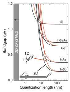
[Category: 2D Crystal Materials and Devices]
·
Get
the preprints
of papers posted on the arXivs.
·
We
have published in IEEE journals, IEDM/DRC, APL, Science, Nature journals,
Physical Review journals, JAP, Nano Letters, etc.
·
The
complete list of papers below is sorted into categories here:
Highlights of our contributions
to the area of 2D Crystal Materials and Devices
18) 2016: Demonstration of controlled
growth of van der Waals heterostructures by MBE.
17) 2015: Demonstration of a broken gap Esaki-diode
with NDR in a mismatched 2D crystal heterostructure.
16) 2015: Proposal and evaluation of a
very low-power transistor using atomically thin TMD semiconductor
heterostructures (the THIN-TFET).
15) 2015: Identified and evaluated carrier
statistics and quantum capacitance effects in atomically thin gapped
semiconductors.
14) 2014: Demonstrated large-area
epitaxial graphene
nanoribbon FETs with record high current drives.
13) 2014: Demonstration of high-voltage
quasi-layered FETs using the wide-bandgap semiconductor Ga2O3.
12)
2014: Identified and evaluated scattering mechanisms and mobility
limits in atomically thin semiconductors.
11) 2013: Identified and evaluated the advantages
of TMD based low-power Tunneling FETs.
10) 2013: First evaluation of Zener
tunneling in TMD semiconductors.
9) 2013: Proposal of the SymFET:
a novel graphene tunneling transistor.
Experimentally verified.
8) 2012: First
demonstration of TMD semiconductor transistors with current saturation and
inversion in multilayer MoS2 FETs.
7) 2012: Prediction of strong
room-temperature NDR in
graphene-insulator-graphene tunnel junctions.
Experimentally verified.
6) 2012: Demonstration of broadband
THz modulators using graphene.
5) 2010: Study of the effect of remote
phonon scattering from high-K dielectrics on mobility in layered materials.
4) 2008: First evaluation
of Zener tunneling in GNRs, and the first proposal and evaluation
of the GNR Tunneling-FET (GNR TFET).
3) 2008: First evaluation of LER
scattering and mobility
in Graphene Nano Ribbons.
2) 2007: First prediction
of the strong effect of dielectric environment on transport in 2D crystal
semiconductors. Experimentally verified.
1) 2007: Evaluated
the carrier statistics and quantum capacitance in graphene/Dirac materials and
nanoribbons. Experimentally
verified.
2016
186) Two-Dimensional
Semiconductors for Transistors
(M. Chhowalla, D. Jena, and H. Zhang,
Nature Reviews, 1, 1-15 2016)
185) Layered
transition metal dichalcogenides: promising near-lattice-matched substrates for
GaN growth
(P. Gupta, et al.,
Nature Scientific Reports, 6, srep23708 2016)
(J. H. Park et al.,
ACS Nano, 10, 4258 2016)
183) Room
temperature weak ferromagnetism in SnxMn1-xSe2 2D films
grown by molecular beam epitaxy
(S. Dong, et al.,
APL Materials, 4, 032601 2016)
179) Controllable
growth of layered selenide and telluride heterostructures and superlattices
using MBE
(S. Vishwanath et al.,
J. Mat. Res., 31, 900 2016)
2015
172) Esaki
Diodes in van der Waals Heterojunctions with Broken-Gap Energy Band Alignment
(R. Yan et al.,
Nano Letters,
15, 5791 2015)
(S. Vishwanath et al.,
2D Materials, 2, 024007 2015)
165) Anisotropic
Thermal Conductivity in Single-Crystal beta-Gallium Oxide
(Z. Guo et al.,
Appl.
Phys. Lett., 106, 111909 2015)
163) 2-dimensional
heterojunction interlayer tunneling FETs (Thin-TFETs)
(M. Li et al.,
IEEE J.
Electron Devices Society, 3, 200
2015)
161) Carrier
statistics and quantum capacitance effects on mobility extraction in 2D crystal
FETs
(N. Ma and D. Jena,
2D Materials,
2, 015003, 2015)
160) Synthesized
multiwall MoS2 nanotube and nanoribbon FETs
(S. Fathipour et al,
Appl.
Phys. Lett., 106, 022114, 2015)
159) Graphene
nanoribbon FETs on wafer-scale epitaxial graphene on SiC substrates
(W. Hwang et al,
APL
Materials, 3, 011101, 2015)
2014
158) 2D
Crystal Semiconductors: Intimate Contacts (News & Views)
(D. Jena, K. Banerjee, H. Xing
Nature
Materials, 13, 1076 2014)
156) Exfoliated
MoTe2 Field-Effect Transistors
(S. Fathipour et al,
Appl. Phys. Lett., 105, 192101, 2014)
152) High-performance
photocurrent generation from 2D WS2 FETs
(S. H. Lee, D. Lee, W.-S. Hwang, E.
Hwang, D. Jena, and W. J. Yoo,
Appl. Phys. Lett., 104, 193113, 2014)
147) Charge
Scattering and Mobility in Atomically Thin Semiconductors
(N. Ma and D. Jena,
Phys.
Rev. X, 4, 011043 2014)
146) High-Voltage
Field-Effect Transistors with Wide-Bandgap Ga2O3
Nanomembranes
(Wan Sik Hwang et al.,
Appl. Phys. Lett., 104, 203111, 2014)
145) A
Computational Study of Metal-Contacts to Monolayer Transition-Metal
Dichalcogenide Semiconductors
(J. Kang, W. Liu, D. Sarkar, D.
Jena, and K. Banerjee,
Phys.
Rev. X, 4, 031005, 2014)
(M. Li et al.,
J. Appl. Phys. 115, 074508 2014)
(Wan Sik Hwang et al.,
J.
Vac. Sci. Technol (b), 32,
012202 2014)
2013
133) High-Performance
Few-Layer-MoS2 Field-Effect-Transistor with Record Low
Contact-Resistance
(W. Liu et al.,
IEDM Tech. Digest, 13, 499 2013)
132) Novel
Logic Devices based on 2D Crystal Semiconductors: Opportunities and Challenges
(D. Jena et al.,
IEDM Tech. Digest, 13, 487 2013)
(H-Y. Chang, et al.,
ACS Nano, 7, 5446, 2013)
127) Tunneling
Transistors based on Graphene and 2D Crystals
(D. Jena,
Proceedings
of the IEEE, 101, 1585, 2013)
126) Graphene
reconfigurable THz optoelectronics
(B. Sensale-Rodriguez, et al.,
Proceedings
of the IEEE, 101, 1705, 2013)
125) Interband
tunneling in 2D crystal semiconductors
(N. Ma and D. Jena,
Appl. Phys. Lett., 102, 132102, 2013)
124) Role
of metal contacts in designing high-performance n-type WSe2 FETs
(W. Liu, et al.,
Nano Lett., 13, 1983, 2013)
122) Graphene
as transparent electrode for direct observation of hole
photoemission from silicon to oxide
(R. Yan et al.,
Appl. Phys. Lett., 102, 123106 2013)
121) Electrical
noise and transport properties of graphene
(N. Sun, et al.,
J. Low. Temp.
Phys., 172, 202 2013)
120) Exciton
dynamics in suspended monolayer and few-layer MoS2 2D crystals
(H. Shi, et al.,
ACS
Nano, 7, 1072, 2013)
117) SymFET:
A proposed symmetric graphene tunneling field-effect transistor
(P. Zhao et al.,
IEEE
Trans. Electron Dev., 60, 951,
2013)
116) Comparative
study of chemically synthesized and exfoliated multilayer MoS2
field-effect transistors
(Wan-Sik Hwang et al.,
Appl. Phys. Lett., 102, 043116, 2013)
113) Terahertz
imaging employing graphene modulator arrays
(B. Sensale-Rodriguez, et al.,
Opt. Exp.,
21, 2324, 2013)
2012
111) High-Mobility,
Low-Power Thin-Film Transistors based on multilayer MoS2 crystals
(S. Kim et al.,
Nature
Comm., 3, 1011, 2012)
110) Broadband
Graphene Terahertz Modulators enabled by Intraband Transitions
(B. Sensale-Rodriguez, R. Yan, M.
Kelly, T. Fang, K. Tahy, W. S. Hwang, D.
Jena, L. Liu, and H. Xing,
Nature
Comm., 3, 780, 2012)
109) Multilayer
Transition Metal Dichalcogenide Channel Thin-Film Transistors
(E. S. Kim et al.,
IEDM Tech. Digest, 12, 108 2012)
108) A
Computational Study of Metal Contacts to Beyond-Graphene 2D Semiconductor
Materials
(J. Kang et al.,
IEDM Tech. Digest, 12, 407 2012)
106) Efficient
THz electro-absorption modulation employing graphene plasmonic structures
(B. Sensale-Rodriguez et al.,
Appl. Phys. Lett., 101, 261115 2012)
105) Graphene
nanoribbon FETs for digital electronics: experiment and modeling
(K. Tahy et al.,
Int. J. of
Circuit Theory, 41, 603, 2012)
103) High-Detectivity
Multilayer MoS2 Phototransistors with Spectral Response from UV to
IR
(W. Choi et al.,
Adv.
Mat., 24, 5832 2012)
101) Extraordinary control of THz beam reflectance in Graphene
electro-absorption modulators
(B. Sensale-Rodriguez et al.,
Nano Lett., 12, 4518, 2012)
(R. Yan, Q. Zhang, W. Li, I. Calizo,
T. Shen, C. Richter, A. Hight-Walker, X. Liang, A. Seabaugh, D. Jena, H. Xing, D. Gundalch, and N.
Nguyen
Appl. Phys. Lett., 101, 022105 2012)
(W.-S. Hwang, M. Remskar, R. Yan, V.
Protasenko, K. Tahy, S. D. Chae, P. Zhao, A. Konar, H. Xing, A. Seabaugh, and D. Jena,
Appl. Phys. Lett., 101, 013107 2012)
(W.-S. Hwang, K. Tahy, X. Li, H.
Xing, A. Seabaugh, C. Y. Sung, and D.
Jena,
Appl. Phys. Lett., 100, 203107, 2012)
90) Fabrication
of Top-Gated Epitaxial Graphene Nano-Ribbon FETs using Hydrogen-silsesquioxane
(HSQ)
(W.-S. Hwang, K. Tahy, L. Nyakiti,
V. Wheeler, R. Myers-Ward, C. Eddy, D. K. Gaskill, H. Xing, A. Seabaugh, and D. Jena,
J. Vac. Sci. Tech. (B), 30(3), 03D14, 2012)
89)
Graphene
(D. Jena,
Springer Encyclopedia (review
article), accepted, to appear, 2012)
88) Single-Particle
Tunneling in Doped Graphene-Insulator-Graphene Junctions
(R. Feenstra, D. Jena, and G. Gu
J. Appl. Phys., 111, 043711, 2012)
2011
80) High-field
transport in two-dimensional graphene
(T. Fang, A. Konar, H. Xing, and D. Jena,
Phys. Rev. B, 84, 125450, 2011)
79) Unique
prospects of graphene-based THz modulators
(S. Sensale-Rodriguez, T. Fang, R.
Yan, M. Kelly, D. Jena, L. Liu, and
H. Xing,
Appl. Phys. Lett., 99, 113104, 2011)
(A. Konar, T. Fang, and D. Jena,
Phys. Rev. B, 84, 085422, 2011)
76) Studies
of Intrinsic Hot Phonon Dynamics in Suspended Graphene by Transient Absorption
Microscopy
(B. Gao, G. Hartland, T. Fang, M.
Kelly, D. Jena, H. Xing, and L.
Huang,
Nano Lett., 11 3184, 2011)
75)
Thermally-limited
current carrying ability of graphene nanoribbons
(A. Liao, J. Wu, X. Wang, K. Tahy, D. Jena, H. Dai, and E. Pop,
Phys. Rev. Lett.,
106, 256801 2011)
(P. Zhao, Q. Zhang, D. Jena, and S. Koswatta,
IEEE
Trans. Electron Devices, 58(9),
3170 2011)
2010
59) Effect
of high-K dielectrics on charge transport in graphene-based field-effect
transistors
(A. Konar, T. Fang, & D.
Phys. Rev. B, 82, 115452, 2010)
55) Quantum
Transport in Graphene Nanoribbons patterned by Metal Masks
(C. Lian, K. Tahy, T. Fang, G. Li,
H. Xing, and D. Jena
Appl. Phys. Lett., 96, 101309, 2010)
2009
51) Hydrodynamic
instability of confined two-dimensional electron flow in semiconductors
(W. R. C-Munoz, D. Jena, & M. Sen
J. Appl. Phys., 106, 014506, 2009)
48) A
Theory for the High-Field Current Carrying Capacity of 1D Semiconductors
(D.
J. Appl. Phys., 105, 123701, 2009)
47) Heat
Transport Mechanisms in Superlattices
(Y. K. Koh, Y. Cao, D. Cahill, &
D.
Adv. Funct.
Materials, 19, 610, 2009)
2008
46) Graphene
Nanoribbon Tunnel Transistors
(Q. Zhang, T. Fang, A. Seabaugh, H.
Xing, & D.
IEEE
Electron Device Lett., 29 (12),
1344, 2008)
45) Mobility
in Semiconducting Graphene Nanoribbons: Phonon, Impurity, and Edge Roughness
Scattering
(T. Fang, A. Konar, H. Xing, & D.
Phys.
Rev. B, 78, 205403, 2008)
43) Zener
Tunneling in Semiconducting Nanotube and Graphene Nanoribbon p-n Junctions
(D.
Appl. Phys. Lett., 93, 112106, 2008)
33) Photocurrent
Polarization Anisotropy of Randomly Oriented Nanowire Networks
(Y. Lu, V. Protasenko, D.
Nano.
Lett., 8, 1352, 2008)
2007
30) Tailoring
the carrier mobility in semiconductor nanowires by remote dielectrics
(A. Konar & D.
J. Appl. Phys., 102, 123705, 2007)
(A. Singh, X. Li, G. Galantai, V.
Protasenko, M. Kuno, H. Xing, & D.
Nano
Lett., 7 (10), 2999, 2007)
26) Carrier
Statistics and Quantum Capacitance in Graphene Sheets and Ribbons
(T. Fang, A. Konar, H. Xing & D.
Appl. Phys. Lett., 91, 092109, 2007)
25) Hydrodynamic
instability of one-dimensional electron flow in semiconductors
(W. R. C-Munoz, M. Sen & D.
J. Appl. Phys., 102, 023703, 2007)
(R. Zhou, H.-C. Chang, V.
Protasenko, M. Kuno, A. Singh, D.
J. Appl. Phys., 101, 073704, 2007)
21) Enhancement
of carrier mobility in semiconductor nanostructures by dielectric engineering
(D.
Phys. Rev. Lett.,
98, 136805, 2007) [In the News
– a) NanoTech,
b) Also featured in the Virtual
Journal of Nanoscale Science and Technology]
2006
14) Ultrathin
CdSe Nanowire FETs and their Optical Properties
(A. Khandelwal, D.
J. Electron. Mat.,
35, 170, 2006)
2005
2004
As a
graduate student @ UC Santa Barbara (Fall
1998 - Spring 2003)
2003
2002
2001
2000